Head: Karel Jurek
The Laboratory of scanning electron microscopy and X-ray microanalysis is an all Institute service center. It is equipped by electron probe X-ray microanalyzer JXA-733 of JEOL (Japan). This instrument is based on scanning electron microscope equipped with three wave-length dispersive spectrometers (WDS) and one energy-dispersive spectrometer (EDS) of Kevex, U.S.A. Software is from SAMx, France. This instrument enables observation of samples in secondary and back scattered electrons modes with resolution up to 7 nm, qualitative and quantitative analysis of chemical elements in the range B – U with resolution about 1µm based on X-ray emission spectroscopy (EPMA – Electron Probe Micro Analysis) and creating X-ray maps (X-ray images). The instrument is equipped also by attachment for Back Scattered Electrons Diffraction (EBSD) of EDAX-TSL, U.S.A., enabling to determine the local orientation of crystals and crystal orientation mapping of polycrystalline samples. For the use in the field of semiconductor research this instrument enables imaging in the Electron Beam Induced Currents (EBIC) mode.
In department of structure analysis the mostly used service is the elemental microanalysis. At analysis of the structure of crystalic materials it is ofen doubtfull if a specific element is present in the sample and in such a case the elemental analysis with the electron microprobe can solve the problem in very short time.
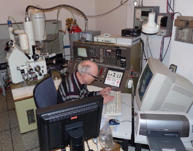
Laboratory of scanning electron microscopy.
Copyright © 2008-2014, Fyzikální ústav AV ČR, v. v. i.


