The research team focuses on the study of electronic and optical phenomena at surfaces and interfaces of nanomaterials caused by the impact of photons, ions, electrons and adsorption of gases for sensor applications, for the development of sources of light, and for the enhancement of the nano-diagnostic capabilities of analytical methods.
Schottky contact is one of the key structures in semiconductor devices. Mechanism of formation of Schottky contacts on compound semiconductors has been the subject of long term investigation. High density of surface states and nonstoichiometric defects in compound semiconductors impedes the preparation of high quality Schottky diodes and substantially restricts the application potential of those materials.
Novel techniques of the preparation of thermally stable Schottky diodes have been developed by using the deposition of colloidal graphite and the electrophoretic deposition of metal nanoparticles (NPs). Our focus is on the theoretical and experimental analysis of the graphite/semiconductor and metal nanoparticles/semiconductor structures.
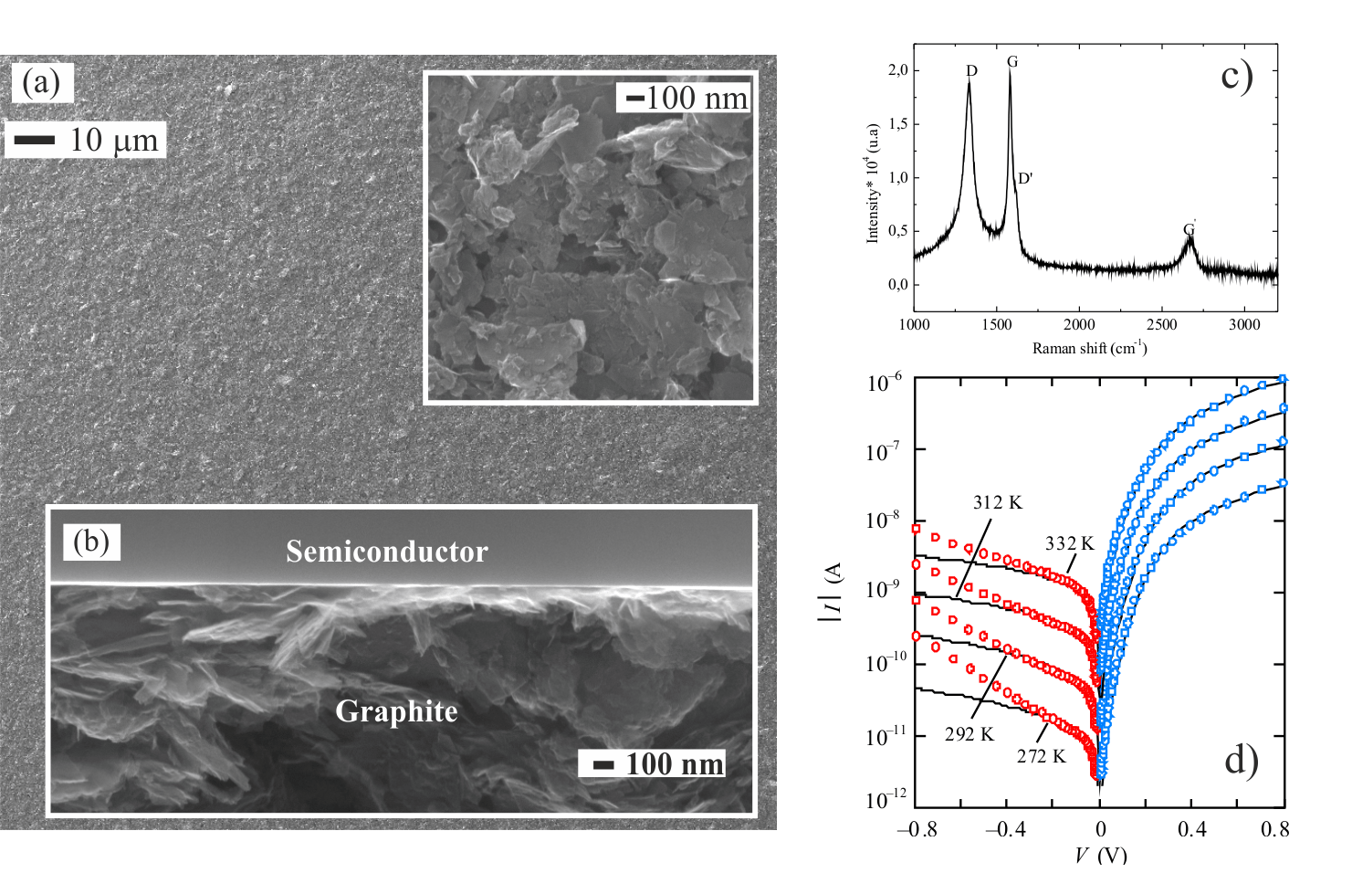
Figure 1: (a) SEM images of the graphite contact deposited on semiconductor substrate; (b) Cross section of the graphite/semiconductor Schottky diodes; (c) Raman spectrum of the graphite; (d) Comparison of the calculation results (solid lines) with the I-V characteristics of graphite/CdMnTe diode measured at different temperatures (circles).
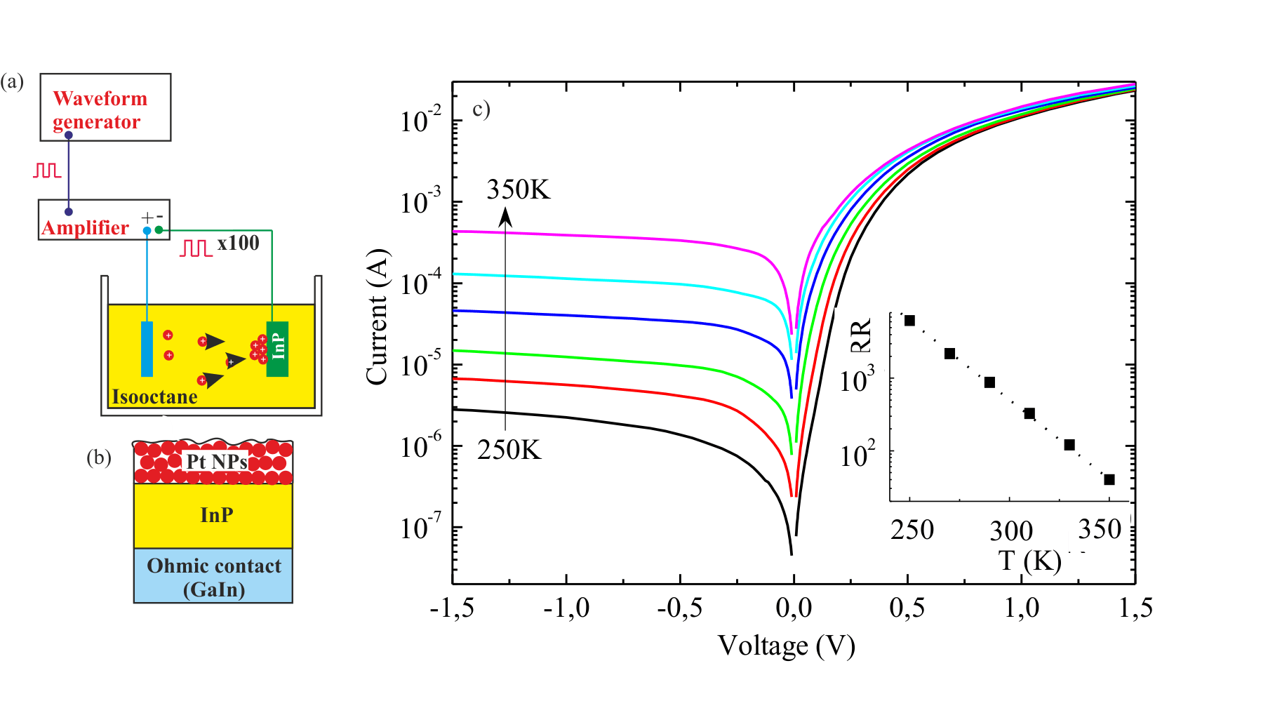
Figure 2: (a) Set-up of the electrophoretic deposition process; (b) Schematic cross-section of Pt NP/InP Schottky diodes; (c) I-V characteristics of the Pt NP/n-InP junctions in a semilogarithmic system of coordinates. The inset shows the temperature dependence of the rectification ratio determined at applied bias of 1V.
Relevant publications:
Hydrogen is nowadays widely used in medicine, chemical or automotive industry and is considered as a fuel of the future with a potential for the substitution of fossil fuels. However, it is highly volatile, extremely combustible, and its leak may cause explosion. Therefore, the development of hydrogen sensors with high sensitivity, short response time, low dimensions, and low production costs is of primary focus.
We have developed hydrogen sensors based on Schottky diodes fabricated by the deposition of colloidal graphite onto semiconductor surfaces functionalized with catalytic nanoparticles (Pt, Pd). These sensors are capable of detecting hydrogen in low concentrations down to 1 ppm.
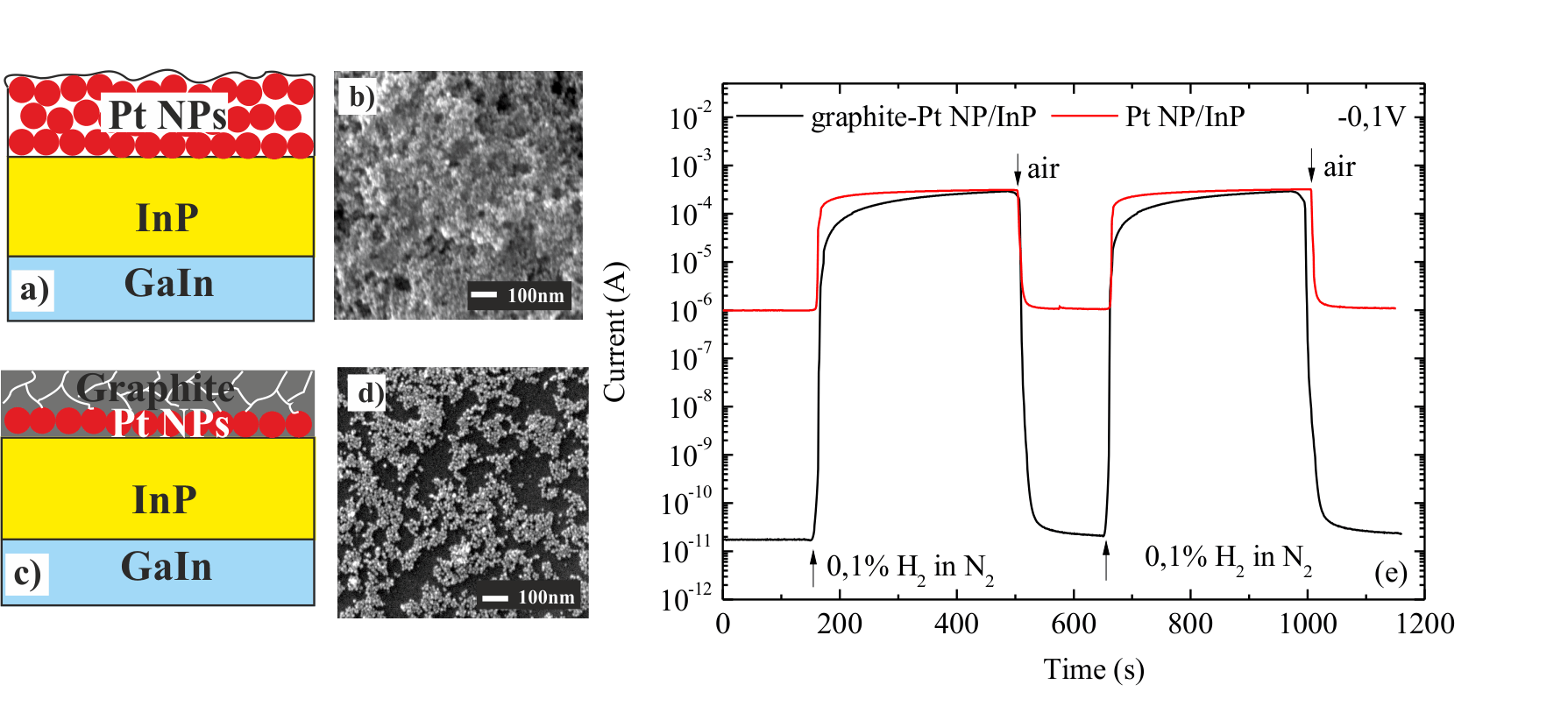
Figure 3: Schematic cross-section of (a) Pt NP/InP and (c) graphite- Pt NP/InP Schottky diodes; SEM images of (b) thick layer and (d) submonolayer Pt NPs deposited on a semiconductor substrate by EPD; (e) Current transient characteristics of the graphite-Pt NP/ InP and Pt NP/InP the Schottky diodes under exposure to hydrogen.
Relevant publications:
Low dimensional semiconductor structures have been intensively studied for prospective electronic and photonic applications. One of the key issues in these devices is to understand and control the charge transport at metal/semiconductor nanostructure interface. Our goal is to describe fundamental phenomena taking place during the charge transport in Schottky barriers prepared on one-dimensional ZnO nanostructures. Vertical arrays of ZnO nanorods (NRs) and nanowires (NWs) are characterized by a set of diagnostic methods as a feedback for the modification of technology in order to tailor their morphology and their electrical, optical, and structural properties. Schottky contacts to individual NRs and NWs and their arrays are formed by vacuum evaporation of metals, by the deposition of colloidal graphite, by e-beam lithography, by focused electron/ion beam induced deposition, and by the tip of atomic force microscope or by the nanomanipulator tip in the scanning electron microscope.
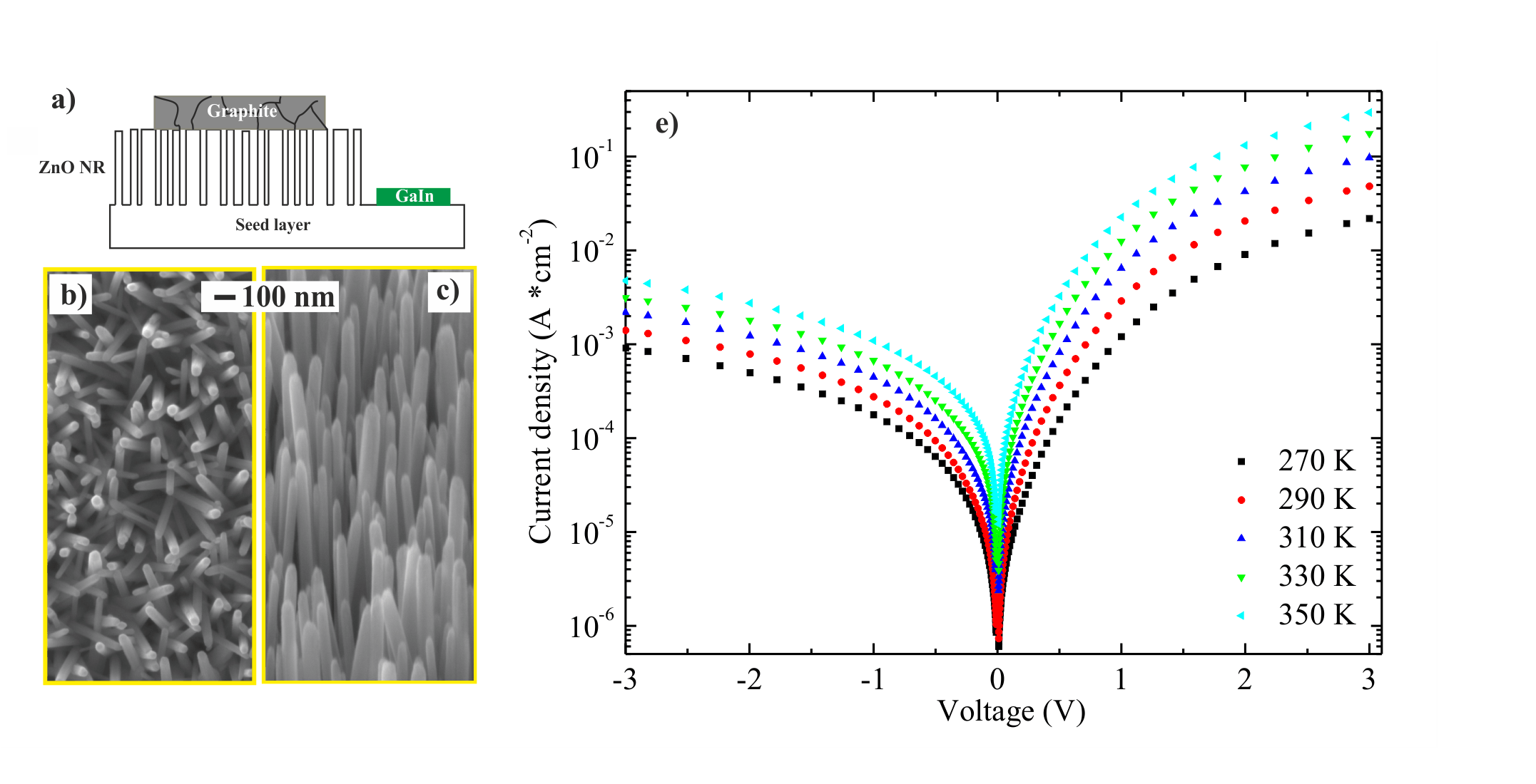
Figure 4: Heterojunction graphite/ZnO NRs: (a) Schematic diagram; (b) top view SEM image of the ZnO NRs; (c) SEM image of the ZnO NRs taken at 55° tilt; (e) I-V curves at different temperatures demonstrating the rectifying behavior of the heterojunction.
Relevat publications:
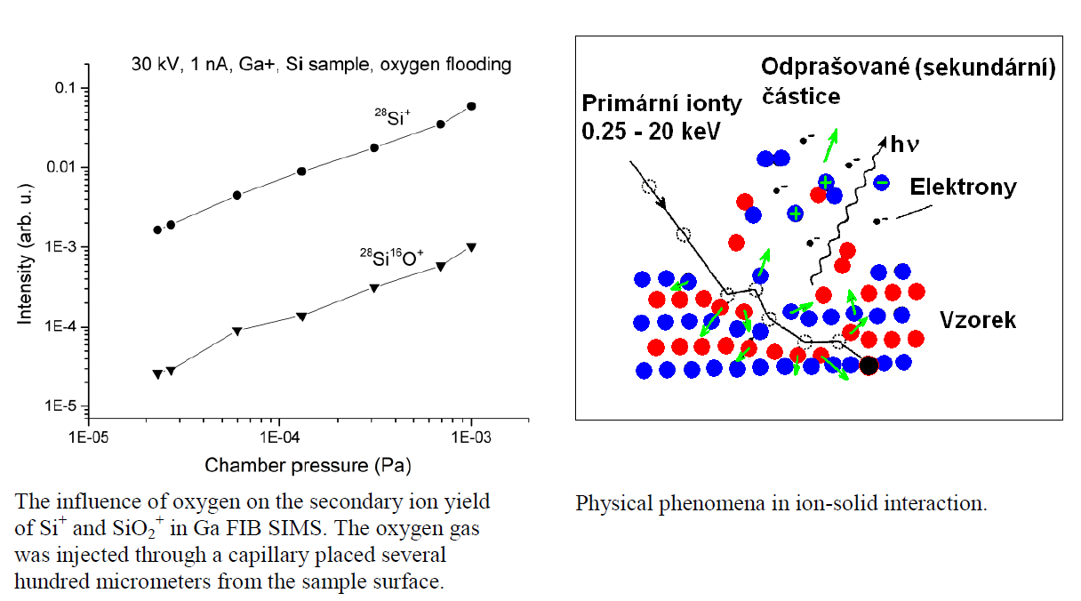
Ion beams are utilized both for the formation of nanostructures and for the chemical analysis of solid surfaces. We study physical and chemical processes initiated by ion bombardment of solid surfaces: sputtering, electron emission, implantation, ionization, formation of nanostructures. We influence those processes by injection of reactive gases, e.g., by oxygen. The understanding of those phenomena is important for correct interpretation of microscopic images of FIB and SIMS, for the improvement of analytical parameters of the SIMS technique or of its modern FIB SIMS variant, and for the development and exploitation of ion-induced formation of nanostructures.
Relevant publications:
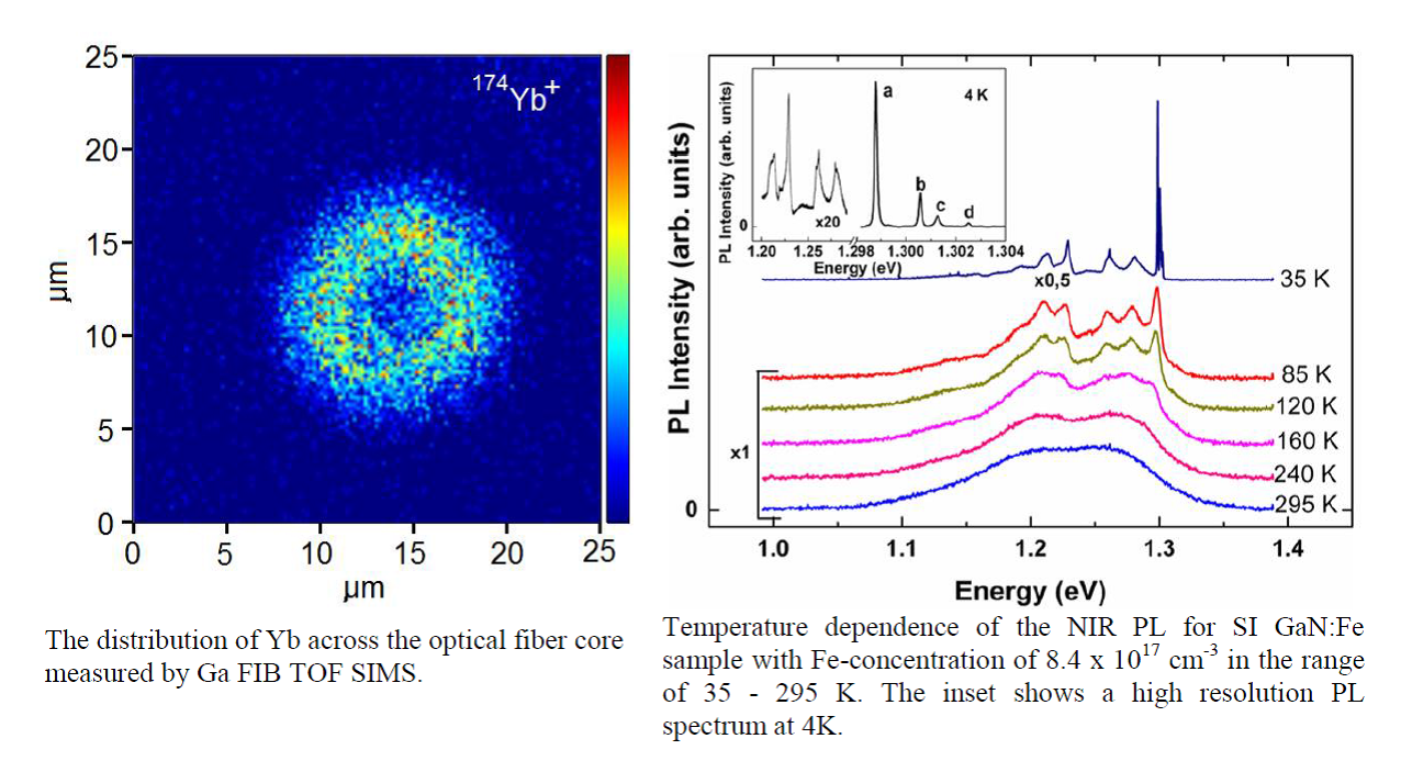
For characterization of the studied materials we have a wide palette of analytical and microscopic techniques available at our institute - SEM, FIB, SIMS, EDX, AFM, STM, BEEM/BEES, Raman spectroscopy, optical microscopy, photoluminescence, cathodoluminescence, where three of them - BEEM/BEES, low temperature photoluminescence, and FIB SIMS we develop, improve or study in more detail. Additionally, in collaboration with other research teams at IPE or AS CR we exploit novel analytical methods targeted to the analysis of optical fibers, special glasses and semiconductor structures.
Relevant publications:
IPE carries out fundamental and applied research in the scientific fields of photonics, optoelectronics and electronics. In these fields, IPE generates new knowledge and develops new technologies.