The research team designs, prepares, and characterizes semiconductor materials and nanostructures, with a focus on advancing the understanding of growth mechanisms, the development of new growth methods, and the elucidation of electrical and optical phenomena taking place at their surfaces and interfaces. This research provides the basis for the development of novel electronic and optoelectronic devices, including light sources and detectors, gas sensors, and sources of green energy.
Preparation of semiconductor nanomaterials
The synthesis of nanoscale building blocks of controllable dimensions, morphologies, and materials is central to nanoscience and nanotechnology. We focus on the preparation of semiconductor nanowires and nanorods from solutions with the goal to tailor their physical, chemical, and electronic properties for specific applications. This is conventionally achieved via a tedious empirical cook and look approach. We go considerably beyond this approach by performing modeling of chemical and physical phenomena taking place in growth solutions, by identifying the nucleation and growth mechanisms, and by developing new growth methods and patterning techniques.

Publications:
- O. Černohorský, J. Grym, H. Faitova, N. Bašinová, Š. Kučerová, R. Yatskiv, and J. Veselý, "Modeling of Solution Growth of ZnO Hexagonal Nanorod Arrays in Batch Reactors," Crystal Growth & Design 20, 3347−3357 (2020).
- N. Basinova, O. Cernohorsky, J. Grym, S. Kucerova, H. Faitova, R. Yatskiv, J. Vanis, J. Vesely, J. Maixner, "Highly Textured Seed Layers for the Growth of Vertically Oriented ZnO Nanorods," Crystals 9 (11), 566 (2019).
- O. Cernohorsky, J. Grym, R. Yatskiv, V. H. Pham, and J. H. Dickerson, "Insight into Nanoparticle Charging Mechanism in Nonpolar Solvents to Control the Formation of Pt Nanoparticle Monolayers by Electrophoretic Deposition," ACS Appl Mater Inter 8 (30), 19680-19690 (2016).
Electric charge transport in semiconductor materials and nanostructures
Understanding charge transport in semiconductor materials and heterojunctions is essential for the design of electronic and optoelectronic devices. In addition to investigating charge transport in bulk semiconductors and ensembles of nanostructures, we develop methods for the in-situ electrical characterization of individual semiconductor nanostructures and heterostructures with two-dimensional materials. The in-situ measurements show great promise in the characterization of the arrays of nanostructures, where individual nanostructures possess different electrical properties and help identify the phenomena that are behind these differences.

Publications:
- S. Tiagulskyi, R. Yatskiv, H. Faitová, Š. Kučerová, D. Roesel, J. Vaniš, J. Grym, J. Veselý, "Highly Rectifying Heterojunctions Formed by Annealed ZnO Nanorods on GaN Substrates," Nanomaterials 10 (3), 508 (2020).
- S. Tiagulskyi, R. Yatskiv, H. Faitová, Š. Kučerová, J. Vaniš, J. Grym, "Electrical properties of nanoscale p-n heterojunctions formed between a single ZnO nanorod and GaN substrate," Materials Science in Semiconductor Processing 107, 104808 (2020).
- R. Yatskiv, S. Tiagulskyi, J. Grym, "Influence of Crystallographic Orientation on Schottky Barrier Formation in Gallium Oxide," Journal of Electronic Materials 49, 5133–5137 (2020).
- R. Yatskiv, S. Tiagulskyi, J. Grym, "Characterization of Graphite/ZnO Schottky Barriers Formed on Polar and Nonpolar ZnO Surfaces," physica status solidi (a) 216 (2), 1800734 (2019).
- R. Yatskiv and J. Grym, "Influence of the Interaction Between Graphite and Polar Surfaces of ZnO on the Formation of Schottky Contact," Journal of Electronic Materials 47 (9), 5002-5006 (2018).
- R. Yatskiv, J. Grym, V. V. Brus, O. Cernohorsky, P. D. Maryanchuk, C. Bazioti, G. P. Dimitrakopulos, and P. Komninou, "Transport properties of metal-semiconductor junctions on n-type InP prepared by electrophoretic deposition of Pt nanoparticles," Semicond Sci Tech 29 (4) (2014).
- R. Yatskiv, V. V. Brus, M. Verde, J. Grym, and P. Gladkov, "Electrical and optical properties of graphite/ZnO nanorods heterojunctions," Carbon 77, 1011-1019 (2014).
- R. Yatskiv and J. Grym, "Temperature-dependent properties of semimetal graphite-ZnO Schottky diodes," Appl Phys Lett 101 (16) (2012).
Optical characterization of materials and nanostructures
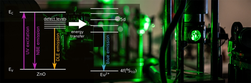
We investigate the optical properties of a broad range of materials including semiconductors, ceramics, and glasses doped with rare-earth ions. The laboratory of photoluminescence spectroscopy is equipped with a unique setup designed and assembled by the team members, which enables sensitive and high-resolution measurements across broad spectral (300-9000 nm) and temperature (3.5-300 K) ranges.

Publications:
- P. Kostka, R. Yatskiv, J. Grym, J. Zavadil, “Luminescence, up-conversion and temperature sensing in Er-doped TeO2-PbCl2-WO3 glasses” Journal of Non-Crystalline Solids 551, 120287 (2021).
- A. V. Vasin, S. Muto, Y. Ishikawa, D. V. Kysil, S. V. Sevostianov, O. F. Isaieva, G. Yu Rudko, R. Yatskiv, S. Starik, V. A. Tertykh, A. N. Nazarov, and V. S. Lysenko, "Evolution from UV emission of phenyl groups to visible emission of pyrolytic nanocarbons dispersed in fumed silica: Alternative insight into photoluminescence of carbon nanodots," Journal of Luminescence 219, 116926 (2020).
- D. Sedmidubský, V. Jakeš, K. Rubešová, P. Nekvindová, T. Hlásek, R. Yatskiv, P. Novák, "Magnetism and optical properties of Yb3Al5O12 hosted Er3+ – experiment and theory," Journal of Alloys and Compounds 810, 151903 (2019).
- R. Yatskiv and J. Grym, "Luminescence properties of hydrothermally grown ZnO nanorods," Superlattice Microst 99, 214-220 (2016).
Nanofabrication
We develop lithographic methods to control the nucleation and growth of one-dimensional semiconductor nanostructures using focused electron and ion beams and scanning probes. The goal is to design techniques for position-controlled deposition of semiconductor nanostructures including lattice-mismatched substrates with nonuniform morphology. We further develop methods for the nanomanipulation of individual nanostructures and for the fabrication of nanoscale electrical contacts.

Publications:
- O. Černohorský, J. Grym, H. Faitova, N. Bašinová, Š. Kučerová, R. Yatskiv, and J. Veselý, "Modeling of Solution Growth of ZnO Hexagonal Nanorod Arrays in Batch Reactors," Crystal Growth & Design 20, 3347−3357 (2020).
- S. Tiagulskyi, R. Yatskiv, H. Faitová, Š. Kučerová, D. Roesel, J. Vaniš, J. Grym, J. Veselý, "Highly Rectifying Heterojunctions Formed by Annealed ZnO Nanorods on GaN Substrates," Nanomaterials 10 (3), 508 (2020).
- S. Tiagulskyi, R. Yatskiv, H. Faitová, Š. Kučerová, J. Vaniš, J. Grym, "Electrical properties of nanoscale p-n heterojunctions formed between a single ZnO nanorod and GaN substrate," Materials Science in Semiconductor Processing 107, 104808 (2020).
Applications of semiconductor nanostructures
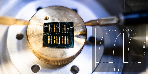
The understanding of the growth phenomena of semiconductor nanostructures together with the unique methods of in-situ electrical characterization of individual nanostructures pave the way for their employment in electronic and optoelectronic devices, including light sources and detectors, gas sensors, and sources of green energy.

Publications:
- R. Yatskiv, S. Tiagulskyi, J. Grym, J. Vaniš, N. Bašinová, P. Horak, A. Torrisi, G. Ceccio, J. Vacik, and M. Vrňata, "Optical and electrical characterization of CuO/ZnO heterojunctions," Thin Solid Films 693, 137656 (2020).
- L. Piliai, D. Tomeček, M. Hruška, I. Khalakhan, J. Nováková, P. Fitl, R. Yatskiv, J. Grym, M. Vorokhta, I. Matolínová, M. Vrňata, "New Insights towards High-Temperature Ethanol-Sensing Mechanism of ZnO-Based Chemiresistors," Sensors 20 (19), 5602 (2020).
- R. Yatskiv, J. Grym, P. Gladkov, O. Cernohorsky, J. Vanis, J. Maixner, and J. H. Dickerson, "Room temperature hydrogen sensing with the graphite/ZnO nanorod junctions decorated with Pt nanoparticles," Solid State Electron 116, 124-129 (2016).
- R. Yatskiv, J. Grym, and M. Verde, "Graphite/ZnO nanorods junction for ultraviolet photodetectors," Solid State Electron 105, 70-73 (2015).
- R. Yatskiv, J. Grym, K. Zdansky, and K. Piksova, "Semimetal graphite/ZnO Schottky diodes and their use for hydrogen sensing," Carbon 50 (10), 3928-3933 (2012).