|
|
|
Close Help | ||||||||||||||
Seminar - Petr Klapetek
14/02/2010 14:00 (Zasedaci mistnost budova B) »more info
Seminar - Guy Le Lay
11/02/2010 11:00 (Seminarni mistnost budova A) »more info
Our paper published in PRL Jan 2011
»more info
Seminar András Berkó
15/11/2010 15:00 (Seminarni mistnost budova A) »more info
Seminar Martin Svec
14/11/2010 15:00 (Seminarni mistnost budova A) »more info
2nd QPlus workshop 8/10/10
2nd International QPlus Workshop 8.10.2010 »more info
Seminar Y. J. Dappe 25/5/10
25/5/2010 10:00 (Seminarni mistnost budova A) »more info
Seminar J. Repp 13/4/2010
14/3/2010 15:00 (Seminarni mistnost budova A) »more info
Seminar T. Novotny 2/3/2010
»more info
Seminar R. Martonak 23/2/10
»more info
4/2/10 Colloquium S. Lindsay
»more info
18/1/10 Our work highlighted on Nanotech.org website.
»more info
30/12/09 Our paper about atomic contrast of KPFM published in PRL
»more info
Seminar J.P. Lewis 9/12/09 14:00
»more info
Seminar P. Kocan 25/11/09 15:00
»more info
14.-15.10. 2009 workshop "Simultaneous STM/AFM measurements using tuning fork based sensors"
»more info
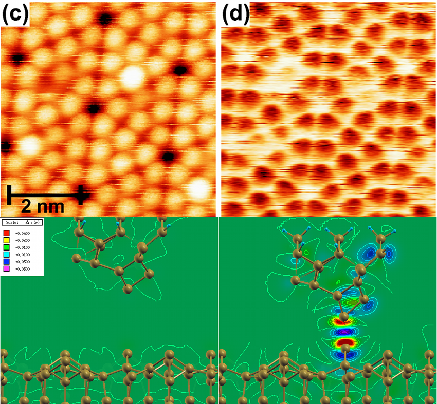
We provide new insight into atomic contrast obtained using Kelvin Probe Force Microscopy based on both experimental and theoretical analysis. We approved, that the atomic contrast is not an artefact, but it has a physical background. In particular, we peform a set of complex computer simulations of tip-sample interaction between a scanning probe and surface. The simulations showed a change of the charge density redistribution and consequently the surface dipole due to the formation of the chemical bond between a probe and surface atoms. This local change round surface atoms is the origin of the atomic contrast observed in the experiment. This work opens new posibilities in characterization of materials at atomic scale.
S. Sadewasser et al. Phys. Rev. Lett. 103, 266103 (2009).
link.aps.org/doi/10.1103/PhysRevLett.103.266103

Fig.
Upper: individual silicon atoms on surface imaged by a traditional nc-AFM topography mode (left) and a new atomic scale image obtained using Kelvin Atomic Force Micorscopy (right). Lower: computer simulations results showing a change in electron density around silicon adatom on surface due to its interaction with scanning probe at different distances, 6,0 Å a 3,5 Å respectivelly.