|
|
|
|||||||||
|
|
|
|
|
|
|
|||||
 |
|
|
||||||||
|
|
 |
 |
Our team is engaged in microlithography technology research with usage of record by an electron-beam writer.
Our work is focused on structures prepared in thin layers either of metals or dielectrics deposited on silicon wafers for different types of sensors.
As for optical applications we design large area microstructures to shape the laser beam and diffraction structures for using in industrial holography.
Fundamental part of research is a solution of exposure control software with respect to processing a large amount of data. One partial solution is the data modelling, the data simulation and parameter optimisation of designed structures and their design simplification. It is also necessary to minimize unwanted device characteristics e.g. proximity effect, structure dimensions distortion due to aberration or thermal drifts. Electron –beam writer is a recording device with a very high resolution (the resolution compared with a high quality laser printer, is some thousand times better). The structures for light beam shaping are one the interesting applications. Although the tiny structure is not visible, one can observe its manifestation when illuminated by a light beam. |
|
||||||
 |
|
|||||||||
 |
|
|||||||||
 |
|
|||||||||
 |
|
|||||||||
 |
|
|||||||||
|
|
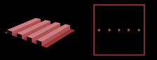
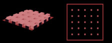
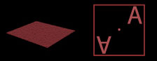
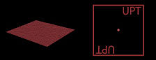
The next model shows gratings with the same spacing as the model from the first figure. In this case however, the orientation of lines is perpendicular to the orientation from the first model. The model shows, that the incident light beam is diffracted at the same rate. But the direction of the deflection is perpendicular to the direction from the first model. Thus, the direction of deflection light beam is related to lines orientation of the grating. One can note that light deflection is perpendicular to the orientation of grating lines.
|
|
 |
|
||||||
 |
|
|||||||||
|
|
|
|||||||||
|
|
|
|
||||||||