|
|
|
Close Help | ||||||||||||||
|
|
|
|||||||||
|
|
|
|
|
|
|
|||||
 |
|
|
||||||||
|
|
 |
 |
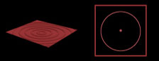
Our team is engaged in microlithography technology research with usage of record by an electron-beam writer.
Our work is focused on structures prepared in thin layers either of metals or dielectrics deposited on silicon wafers for different types of sensors.
As for optical applications we design large area microstructures to shape the laser beam and diffraction structures for using in industrial holography.
Fundamental part of research is a solution of exposure control software with respect to processing a large amount of data. One partial solution is the data modelling, the data simulation and parameter optimisation of designed structures and their design simplification. It is also necessary to minimize unwanted device characteristics e.g. proximity effect, structure dimensions distortion due to aberration or thermal drifts. Electron –beam writer is a recording device with a very high resolution (the resolution compared with a high quality laser printer, is some thousand times better). The structures for light beam shaping are one the interesting applications. Although the tiny structure is not visible, one can observe its manifestation when illuminated by a light beam. |
|
||||||
 |
|
|||||||||
 |
|
|||||||||
 |
|
|||||||||
 |
|
|||||||||
 |
|
|||||||||
|
|
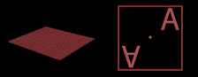
Another example of a general structure that is different from the last case. A human sight is not able to recognize recorded information (respectively the difference from last case). But diffraction patterns are in both cases distinguishable. Note that structures of this type were usually prepared naturally by an interferential holography. The final structure of a holographic record is called the hologram. One simple definition might be: the hologram is a record of image space frequencies. In our case, the structure is created by an exposure in an electron-beam writer without using the light beam. In order to distinguish such structures we call them the synthetic hologram.
|
|
 |
|
||||||
 |
|
|||||||||
|
|
|
|||||||||
|
|
|
|
||||||||