|
|
|
Close Help | ||||||||||||||
|
|
|
|||||||||
|
|
|
|
|
|
|
|||||
 |
|
|
||||||||
|
|
 |
 |
Our team is engaged in microlithography technology research with usage of record by an electron-beam writer.
Our work is focused on structures prepared in thin layers either of metals or dielectrics deposited on silicon wafers for different types of sensors.
As for optical applications we design large area microstructures to shape the laser beam and diffraction structures for using in industrial holography.
Fundamental part of research is a solution of exposure control software with respect to processing a large amount of data. One partial solution is the data modelling, the data simulation and parameter optimisation of designed structures and their design simplification. It is also necessary to minimize unwanted device characteristics e.g. proximity effect, structure dimensions distortion due to aberration or thermal drifts. Electron –beam writer is a recording device with a very high resolution (the resolution compared with a high quality laser printer, is some thousand times better). The structures for light beam shaping are one the interesting applications. Although the tiny structure is not visible, one can observe its manifestation when illuminated by a light beam. |
|
||||||
 |
|
|||||||||
 |
|
|||||||||
 |
|
|||||||||
 |
|
|||||||||
 |
|
|||||||||
|
|
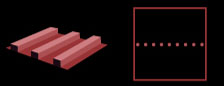
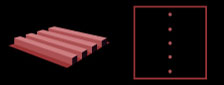
An observable diffraction occurs during incidence of light with a fine regular grating. The light beam does not only reflect in the direction given by the reflection from structure plane but also in other directions. The figure represents a 3D model of an experiment, when the diffraction occurs on grating. The light source is on the left, the diffraction grating is down and the light image coming to a screen is on the right. The parallel beam of light from the source incidents on the grating and there it is reflected and diffracted in different directions. The highlighted (red) points on the screen represent areas, where the intensity of light is the highest. These points are called the diffraction maxima.
|
|
 |
|
||||||
 |
|
|||||||||
|
|
|
|||||||||
|
|
|
|
||||||||