|
|
|
Close Help | ||||||||||||||
|
|
|
|||||||||
|
|
|
|
|
|
|
|||||
 |
|
|
||||||||
|
|
 |
 |
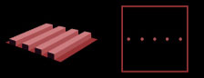
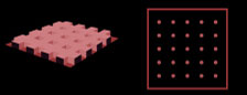
Our team is engaged in microlithography technology research with usage of record by an electron-beam writer.
Our work is focused on structures prepared in thin layers either of metals or dielectrics deposited on silicon wafers for different types of sensors.
As for optical applications we design large area microstructures to shape the laser beam and diffraction structures for using in industrial holography.
Fundamental part of research is a solution of exposure control software with respect to processing a large amount of data. One partial solution is the data modelling, the data simulation and parameter optimisation of designed structures and their design simplification. It is also necessary to minimize unwanted device characteristics e.g. proximity effect, structure dimensions distortion due to aberration or thermal drifts. Electron –beam writer is a recording device with a very high resolution (the resolution compared with a high quality laser printer, is some thousand times better). The structures for light beam shaping are one the interesting applications. Although the tiny structure is not visible, one can observe its manifestation when illuminated by a light beam. |
|
||||||
 |
|
|||||||||
 |
|
|||||||||
 |
|
|||||||||
 |
|
|||||||||
 |
|
|||||||||
|
|
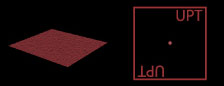
This structure is more general than the previous examples. This structure is designed to bend the incident light into selected directions. Selected directions are bound by the profile of a letter A. The diffraction pattern is symmetrical with respect to the central point, similarly to the past examples. Organization of structure (the way of its modulation) is not as simple. (Note that a 2D Fourier transformation is used for calculations).
|
|
 |
|
||||||
 |
|
|||||||||
|
|
|
|||||||||
|
|
|
|
||||||||